Research Article | | Peer-Reviewed

A Review of ZnO Wide-Bandgap Semiconducting Materials and Future Applications

Received: 7 November 2025     Accepted: 18 December 2025     Published: 6 August 2026
Views:       Downloads:
Abstract

We report on water splitting, disinfection, and pollutant degradation processes assisted by photocatalysis supported by zinc oxide (ZnO) under varied experimental and environmental conditions. In addition, the role of ozonation in the presence of ZnO and its synergistic impact on the effective elimination of organic and inorganic contaminants is discussed, highlighting enhanced reaction kinetics and mineralization efficiency. ZnO nanoparticles (ZnO-NPs) have also emerged as appropriate and versatile tools in drug delivery systems and chemical or biological sensing applications due to their biocompatibility, tunable surface chemistry, and strong photoluminescence response. Owing to its distinctive structural, optical, and electronic properties, ZnO has been extensively employed as an n-type inorganic semiconductor in organic solar cells (OSCs) and hybrid solar cells (HSCs), where it functions efficiently as an electron transport and hole-blocking layer. Its high chemical and thermal stability, non-toxicity, facile synthesis routes, low production cost, and excellent optoelectronic characteristics make ZnO highly attractive for large-scale technological applications. Furthermore, ZnO is widely used as a preservative and functional additive in numerous products and materials, including foundations, ceramics, glass, rubbers, lubricants, plastics, cement, ointments, paints, adhesives, sealants, colorants, ferrites, foods, batteries, food enhancers, fire-retardant systems, and first-aid tapes. These diverse applications underscore the multifunctional nature and industrial relevance of ZnO-based materials.

Published in Science Discovery Materials (Volume 1, Issue 2)
DOI 10.11648/j.sdm.20260102.12
Page(s) 71-80
Creative Commons

This is an Open Access article, distributed under the terms of the Creative Commons Attribution 4.0 International License (http://creativecommons.org/licenses/by/4.0/), which permits unrestricted use, distribution and reproduction in any medium or format, provided the original work is properly cited.

Copyright

Copyright © The Author(s), 2026. Published by Science Publishing Group

Keywords

ZnO, Dilute Magnetic Semiconductors, Multifunctional Properties, Rare-Earth Metal

1. Introduction
ZnO material is important for its multi-functional properties. The characteristics of ZnO can modify by doping various elements. ZnO-based dilute magnetic semiconductors doped with transition Metals are anticipated to make excellent candidates. For large magnetization. The Ferromagnetic properties at room temperature of ZnO can be increased by doping Mn, Co, Fe, Ti, and copper elements. As far as doping is concerned, rare-earth metal ions like Er, Tb, etc, lead to the modifying of emission properties of ZnO towards the visible region.
The band gaps of materials influence the properties like electrical, optical, and index of refraction. The groups of II-VI semiconductors are efficient emitters in the blue to ultraviolet (UV) spectral range and are suitable candidates for light emitting laser diodes. The direct band gap semiconductors have more advantages over indirect band gap semiconductors. The directly band gap semiconductors are used in various applications such as ultraviolet light emitting diodes (UV LEDs) and ultraviolet photo-detector .
ZnO has an energy band gap of 3.44 eV at low temperatures and 3.37 eV at room temperature. It has uses in photodetectors, light-emitting diodes, and optoelectronics in the blue/UV range. ZnO has a free-exciton binding energy of 60 meV compared to GaN's 25 meV.
Given its high excitonic binding energy, ZnO may be able to emit effectively at temperatures higher than room temperature. Because excitons frequently have oscillator strengths that are significantly higher than those of direct electron-hole transitions or indirect band gap semiconductors, For optical systems based on excitonic processes, ZnO is a suitable material. Due to its superior piezoelectric and transparent qualities, ZnO stands out among the other semiconducting oxides as a special kind of material. Due to these characteristics, ZnO material is a great choice for window layers and transparent conducting electrodes in solar cell applications. Strong pyro electric and piezoelectric capabilities are produced by the high electromechanical coupling in ZnO and the poor symmetry of the wurtzite crystal structure. ZnO is a useful material for vacuum fluorescent displays and field emission displays due to its intense luminosity in the green-white region of the spectrum. ZnO is helpful as an addition due to its high heat conductivity (e.g. ZnO is added to rubber to increase the thermal conductivity of tires). The availability of a substantial area of single crystals in ZnO makes it the semiconductor with the most alluring properties. Thus, ZnO thin films can be grown epitaxial on ZnO single crystal substrates.
Low-temperature chemical etching gives a great deal of freedom to the manufacturing, designing, and integration of electrical and optoelectronic devices. ZnO thin films may be etched with acidic, alkaline, as well as combination solutions. ZnO has been shown to have an unusually high radiation hardness, even higher than GaN. For use in space or at great altitudes, radiation hardness is crucial.
The main benefit of ZnO over GaN is the availability of massive single crystals. GaN, for instance, is often developed on sapphire, with a significant lattice mismatch of approximately 16% that results in an enormously high dilution of extended defects (106-109 cm2). Managing the conductivity of ZnO has remained a challenging task. Even very low levels of native point defects and impurities (as low as 10-14 cm3 or 0.01 ppm) can have a substantial impact on semiconductors' electrical and optical characteristics. Consequently, the key to regulating the conductivity in ZnO is to understand the role of native point defects (such as vacancies, antisites and interstitials) and the incorporation of impurities. It has long been believed that oxygen positions or zinc interstitials are what produce the unintended n-type conductivity in ZnO.
In addition to structural stability, the green and yellow emissions caused by defects in ZnO have also been thoroughly studied varied forms and dopants can impart varied luminescence capabilities to core-shell nanostructures or quantum dots. In ZnO, defect tuning has received far greater attention, with the majority of the research focusing on stoichiometry for oxygen. In contrast, grain composition, boundary, shape, and lattice characteristics are thought to have less of an influence on the luminescence in ZnO.
2. Core Properties & Why ZnO Matters
ZnO is a direct wide-bandgap oxide semiconductor (Eg ≈ 3.3–3.4 eV) with strong excitonic effects at room temperature, large excitonic binding energy, good electron mobility (especially in high-quality films/nanostructures), piezoelectricity, transparency in the visible, and a rich variety of nanostructured morphologies (wires, rods, films, nanoparticles). These properties make ZnO a model wide-bandgap oxide for UV optoelectronics, transparent/flexible electronics, sensors, piezoelectric nanogenerators and photocatalysis.
3. Crystal Structure
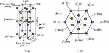
There are three different types of ZnO crystals: the three-dimensional zinc blende, the uncommon cubic rock salt, and the hexagonal wurtzite. Because it has the best stability under typical operating circumstances, the wurtzite structure is the one that is most frequently utilized. Only growth on cubic substrates can maintain the zinc blende ZnO structure, and very high pressures can produce the rock salt NaCl structure. At 3.37 eV at ambient temperature, zinc oxide (ZnO) is a well-known wide band gap semiconductor with a wurtzite structure and lattice parameters of 0.325 nm and 0.5206 nm . ABA is present in the wurtzite structure hexagonal close packing (HCP) structure. The structure of ZnO consists of alternating planes composed of Oí and Zn2+ ions, which are tetrahedrally coordinated and stacked along the c-axis on an alternate basis.
The surface energy is diversified as a result of the normal dipole moment and immediate polarisation that the Zn2+ and O ions produce.
ZnO exhibits piezoelectricity and piezoelectricity as a result of its non-Centro symmetric structure caused by tetrahedral coordination. Polar surfaces are another significant property of ZnO. The basal plane is the most typical polar surface. ZnO are exceptional and cannot be obtained through extensive surface reconstructions. The tetrahedral coordination of this combination is also a typical sign of sp3 covalent bonding, in addition to the inherent polarity of ZnO crystal. ZnO is on the cusp between being categorized as a covalent molecule and an ionic compound since the Zn-O bond also has a very strong ionic property.
4. ZnO Nanostructures
Moreover, nanostructures have attracted increasing interest because of their enhanced physical and chemical properties in the nanoscale regime. “Nanostructure” is a material of interest, that represents a system or object with at least one of its dimensions approximately one hundred nanometres or less. For example, nanorods have one dimension in the nanoscale, i.e. the diameter of the nanorods or less. For example, nanorods have one dimension in the nanoscale, i.e. the diameter of the nanorods is between 1 and 100 nm and its length can be very large in between 1 and 100 nm and its length can be very large.
In the case of a spherical particle, it has all three dimensions between 1 and 100 nm.
The nanostructures can be classified into three categories,
1) dimensional (0D) (e.g. nanoparticles and quantum dots).
2) dimensional (1D) (e.g. nan needle, nanowire, Nanorod, Nano belt).
3) dimensional (2D) (e.g. ultra-thin films).
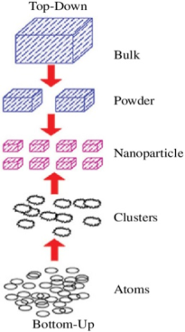
Synthesis and understanding the growth aspects of these nanostructures are important to effectively make nanoscale devices. During the last decade, the growth of Due to its special uses in mesoscale physics and the creation of nanoscale devices, one-dimensional (1D) ZnO nanostructures, such as wires, rods, and tubes, have drawn intense study attention . For the use of 1D nanostructures in a variety of applications, the capacity to accurately regulate or alter their size, chemical composition, surface characteristics, phase purity, and crystal structure has become more crucial. Nanorods made of ZnO are displayed due to their novel properties and potential applications. ZnO nanorods are attractive components for nanometre scale electronic and photonic device applications because of their unique chemical and physical properties. ZnO nanorods have been synthesized by various methods such as the condensation process, template-based growth method, chemical vapour deposition, and wet chemical synthesis. Recently, a wide variety of nanodevices including ultraviolet lasers field effect transistors and light emitting device arrays have been fabricated using ZnO nanorods. Generally, two categories of synthesis and fabrication techniques are used- the Top-down and Bottom-up approaches. A common top-down technique for creating nanoparticles is attrition or milling, but a successful bottom-up technique is colloidal dispersion. The "top-down" method makes use of lithography and finely crafted instruments like cutting, etching, grinding, etc. to create nano scale things from bulk materials. In the ‘bottom-up’ approach, where materials and devices are built from molecular components which assemble themselves chemically using principles of molecular recognition. Atom by atom, molecule by molecule, or cluster by cluster construction is referred to as a bottom-up strategy. The schematic of the top-down and bottom-up approaches is shown in Figure 1.
Figure 1. a) ZnO Unit Cell with Wurtzite Structure. b) Various Crystal Planes of Zn.
5. Challenges and Prospects of ZnO
No precise structures have been proposed clarifying their creation throughout the disclosed techniques, despite the wide range of element sizes, morphologies, and structures that have been devised for manufactured ZnO nano-sized structures. There is still a long way to go before a thorough knowledge of the impacts of the synthesis parameters on particle, structure, size, and morphology has been attained, despite the advances made in studies focusing on the influence of the circumstances of synthesis on the structure and morphology. Because of its advanced electron diffusivity than TiO2, high electron mobility, unusually large exciton binding energy, low cost, and strong endurance against photo-corrosion, ZnO has been regarded as the ideal substitute for TiO2 as the electron transport material in DSSCs and PSCs. Despite this, further research must be done on the effects of ZnO nanostructures' inadequate shape on solar cells' overall efficiency and the related process. The subject of photocatalysis has undergone a revolution because to ZnO nanostructured particles. Additionally, their effectiveness in water splitting and degrading resistant organic water contaminants has been extensively studied and utilised. They still need to address a few worrying features of their photocatalytic activity, perhaps through corrective action. Recently, scientists have paid a lot of attention to ZnO's biological uses.
Currently, efforts are being made to develop more effective ZnO NP applications for drug delivery systems, antibacterial activity, anti-cancer activity, anti-inflammatory activity, anti-diabetic activity, and bio-imaging activity. Recent studies have examined the function of ZnO nano fertiliser in promoting crop growth, yield, and stress. Sadly, the output of staple food crops has not been able to keep up with the pace as the world's population is growing at an alarming rate.
6. Synthesis 1-D Nanostructures
6.1. Aqueous Solution Synthesis Process
Figure 2. Schematic Representation of (a) Top-Down and (b) Bottom-Up Approaches.
At low temperatures, aqueous solution synthesis is frequently utilized to create ceramic materials and oxide nanostructures. This procedure involves gradually raising the temperature of an aqueous solution of metal salts or complexes to below 180°C. Because just water is used as a solvent, such a method does not need high-pressure containers and is also completely recyclable, secure, and environmentally beneficial. With this method, organic solvents' potential toxicity, eventual evaporation, and safety risks are all avoided. By adjusting variables like temperature, precursor concentrations, and pH level, one may fine-tune the morphology of the resultant nanostructures. More crucially, doping occurs during the aqueous chemical development and is normally accomplished by combining the precursors in the proper ratio. Additionally, the materials' purity has significantly increased due to the absence of organic solvents and surfactants. Due to the remaining salts' high solubility, water may remove them with ease. Zinc acetate dihydrated and Ethylene glycol are mixed to achieve the desired solution. Furthermore, different alcohols are added to Zinc and which is proceeded for the oil bath and installed condenser. It is heated up to 160°C and kept for one hour. The calcination takes place at 500°C and is further kept for one hour. It is depicted in Figure 2.
6.2. Sol-Gel Method
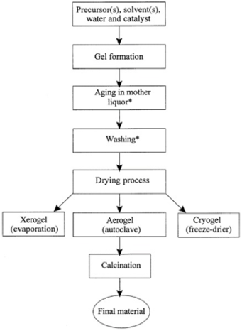
The sol-gel process entails the evolution of inorganic networks by producing a colloidal suspension (sol), and then, as the name suggests (gel), gelating the sol to build a network in a constant liquid phase. The precursors used to create these colloids are composed of a metal or metalloid and a variety of reactive ligands. The most common metal alkali oxides are those that react easily with water. The sol-gel process is often described at the functional group level in terms of three reactions: alcohol condensation, hydrolysis, and water condensation.
Figure 3. Flow Chart of the Materials Derived from Sol-Gel.
Because homogeneity and stoichiometric control are simple using the sol-gel process, it is a flexible technique that can be beneficial for producing metal oxides. It is simple to manufacture materials with excellent quality and. Figure 3 shows the flow chart of the materials derived from the sol-gel method.
6.3. Hydrothermal Synthesis
According to its definition, hydrothermal amalgamation is a part of solvothermal synthesis, which uses water at high pressure. The fundamental idea is that when exposed to high temperatures and pressures, tiny crystals would uniformly nucleate and develop from solution. Water serves as a catalyst as well as a potential component of the solid-state phase at times throughout the nucleation and growth processes. Water frequently becomes supercritical in the harsh circumstances of the amalgamation vessel (autoclave or bomb), reducing its viscosity and enhancing the liquid's dissolving power, diffusivity, and mass transport. A way to customise the density of the finished product is also made possible by the vessel's pressure adjustment capability.
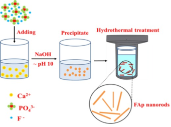
Hydrothermally produced materials are typically single crystals of exceptional quality that come in a variety of sizes and forms. Recently, well-associated ZnO Nanorods on GaN substrates have been created for photosensitive applications via hydrothermal synthesis. The hydrothermal synthesis is shown in Figure 4.
Figure 4. Hydrothermal Synthesis Technique.
6.4. Template Directed Growth
Utilizing template-directed techniques, which use a regularly structured template (such as an anodic alumina membrane or a polymeric membrane) to drive the formation of the material, it is possible to create nanostructures. Other methods, including heat evaporation, can be used to fill the pores of these templates. PLD, or electrodeposition. After the deposition of materials, the templates can be effectively etched out leaving the nanostructures. Nano rods have been obtained by evaporation on a gold membrane. This template-directed approach can be employed to synthesize nanostructures of complex materials, which are otherwise difficult to synthesize by other common methods. In addition to these, several less popular techniques and combinations of these techniques have been employed for the growth of nanostructures.
7. Electrochemical Deposition
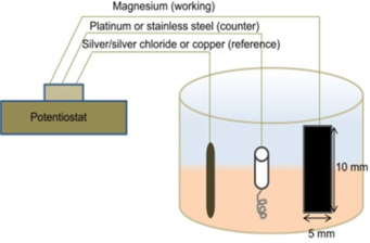
An electrolytic cell made composed of an anode, which is positively charged, a cathode, which is negatively charged, and an electrolyte solution is used in electrodeposition to deposit the thin layer by the flow of electric current. From both aqueous solutions, several different metals, metal alloys, and semiconductor systems have been electroplated successfully. Electroforming, a method that has several industrial uses, allows for the deposition of films ranging in thickness from extremely thin to very thick. It is depicted in Figure 5.
Figure 5. Electrochemical Deposition Technique.
8. Doping in ZnO
ZnO is a significant material for electrical and optoelectronic devices due to its variety of functionalities (magnetic, semiconducting, piezoelectric, etc.). The n-type conductivity of ZnO may be changed by either growing it in an oxygen-deficient environment or by doping it with group III elements like Al, Ga, or In. ZnO is an n-type semiconductor as-grown . Theoretically, it has been predicted that ZnO-based dilute magnetic semiconductors doped with transition metals (Co, Mn) are promising candidates for room temperature ferromagnetism and high magnetization . In addition to these dopants, ZnO can also have its emission properties tailored toward particular wavelengths in the visible region by being doped with luminescent centres like rare-earth metal ions. This is useful for a number of applications, such as multicolored emission in light emitting.
9. Doping of Rare-Earth (RE) Ions in ZnO
Growing ZnO in an oxygen-deficient environment or doping it with group III elements like Al, Ga, or In can both alter its n-type conductivity. As-grown, ZnO is an n-type semiconductor . Theoretically, strong magnetization and room temperature ferromagnetism have been anticipated for ZnO-based dilute magnetic semiconductors doped with transition metals (Co, Mn) . In addition to these dopants, ZnO may also be doped with luminous centres like rare-earth metal ions to tune its emission characteristics toward certain wavelengths in the visible area. Applications for this include multicoloured emission in light emitting diodes. of the potential applications. With the careful selection of the appropriate ion, intense, sharp emission can be obtained across the visible region and into the near-infrared region. The emission peak positions are stable. For these practical advantages, rare earth has been widely utilized in optical applications such as solid lasers and phosphor in color television . Dorenbos and van der observed that the charge transfer level of RE3+ in ZnO is equal to or higher than the bottom of the conduction band of ZnO, which leads to the absence of efficient ZnO RE3+ energy transfer.
In order to avoid concentration quenching, which is particularly harmful to the luminescent features, rare-earth species require extremely high dispersion. Since it is thought that the rare-earth active luminescence centres are located at the grain boundaries, improved device efficiency may be particularly attributed to size-dependent optical characteristics and high grain boundary content in Nanosystems . The light-emitting properties of pure and doped ZnO nanocrystalline films are significantly influenced by the type, amount, and distribution of dopants as well as the degree of crystallinity. For these reasons, the synthesis conditions can have a big impact on the luminescence properties of such systems.
10. Zinc Oxide Thin Films
Since more than a century ago, several materials have been produced as thin films due to their prospective uses and the scientific interest in their characteristics. The two categories of preparation methods are physical process and chemical process. Molecular beam epitaxy, Pulsed laser deposition (PLD), physical vapour deposition (PVD) and sputtering are some of the physical processes involved. The gas-phase methods are chemical vapour deposition (CVD) and atomic layer epitaxy (ALE) while spray pyrolysis spin and dip-coating methods employ precursor solutions. Due to ease and inexpensiveness, chemical techniques have been used broadly for the making of thin films.
11. Preparation of Zinc Oxide
The ZnO thin films can be prepared by many techniques, such as vacuum evaporation, sol-gel sputtering, spray pyrolysis, chemical vapor deposition (CVD), and pulsed laser deposition. The chemical spray pyrolysis has attracted several research groups because of its simplicity, efficiency, and inexpensive technique, and can be widely used for the deposition of large area thin films deposition.
12. Thermal Evaporation
The crucible, source material, and substrate are placed inside the chamber. To increase vapor pressure and its range lies in between 10-2 and 10-9 Torr (ultra-high vacuum).
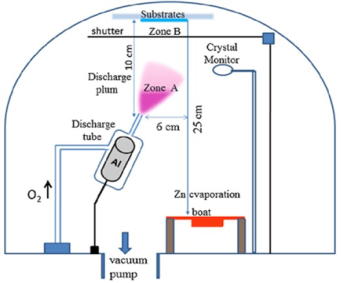
An electron source is directed at the source material during electron-beam evaporation, which results in localized heating. In contrast, RF induction generates an alternating current through an induction coil using an AC power source. Within the coil, the alternating current creates a magnetic field. Localized heat is produced when the source material is placed within the coil because the magnetic field causes eddy currents to form inside the material. It is depicted in Figure 6.
Figure 6. Activated Reactive Evaporation.
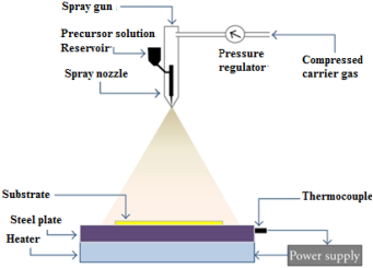
The usual setup for spray pyrolysis consists of an atomizer, precursor solution, substrate heater, and temperature controller. The temperature of the substrate and the precursor solution influence the properties of the films in the spray pyrolysis process.. Spray pyrolysis thin-film deposition may be broken down into three fundamental processes: atomization of the precursor. A film growth model was presented, and the gravitational, electric, thermophoretic, and Stokes forces were also taken into consideration. These forces are responsible for both the trajectory.
The precursor vaporizes at the greatest temperatures (process D), therefore the solid particles are created after the chemical reaction has taken place in the vapour phase. A flexible and efficient method to deposit metal oxide layers is spray pyrolysis. The substrate temperature is the most crucial variable. The films are highly rough and more porous as the substrate temperature is greater. The films will shatter at a low enough temperature. Additionally, the temperature of the substrate affects the physical characteristics such as roughness and crystallinity. Figure 7 shows a schematic illustration of a homemade spray pyrolysis system.
Figure 7. Spray Pyrolysis Technique.
13. Conclusion
This summary explains ZnO is a versatile material with a variety of characteristics, uses, and applications in the developing field of nanotechnology. ZnO NPs may be employed in novel materials and have potential applications in a variety of technological domains due to their high level of high photostability, chemical stability, broad spectrum of radiation absorption, biodegradability, and biocompatibility. Additionally, the development of several bio mediated eco-friendly ZnO particle syntheses with enhanced features that may be modified for their better uses in numerous technological domains has captivated increased attention in them in the globe of study.
The review of recent literature presented here shows that nano- and micrometric zinc oxide particles can be manufactured using a variety of techniques. These can be separated into chemical and metallurgical processes. Zinc oxide is produced in metallurgical operations by roasting a suitable zinc ore, either directly or indirectly. The two categories of chemical methods are condensation methods and dispersion procedures. Zinc oxide is produced in dispersion (mechanochemical) methods by grinding appropriate precursors. The final product can have particles that are around 20 nm in size.
The necessity to restrict the amount of agglomeration and minimize the amount of zinc oxide in particular materials has prompted the development of a number of ZnO surface modification techniques.
According to numerous studies in the literature, depending on how the systems created are to be employed, modification activities can be supported out utilizing inorganic chemicals (oxides and hydroxides), organic substances (alkoxysilanes, carboxylic acids), and specific polymer matrices. Crystalline oxide powders offer opportunities to gain better mechanical, chemical, optical, or electrical properties when mixed with other materials.
One of the scientific and technological fields that is now advancing the most quickly is the study of oxide materials with nano- and micrometric dimensions. Among other things, the usage of such materials can produce catalysts, transparent solar screens that resist infrared and ultraviolet light, and ceramics that are more durable. Additionally, these resources are beneficial for scientific research, disease detection, and therapy. They can be utilized to safely deliver medications to sick cells while avoiding side effects.
According to the review of the research presented here, zinc oxide can be categorized as a multifunctional material. A wide spectrum of radiation absorption, good photostability, a low electrical constant, a high electrochemical coupling index, and excellent chemical stability are among the properties that enable this. It is reasonable to assume that zinc oxide will continue to grow in popularity, opening up new prospects for its application.
Abbreviations

OSCs

Organic Solar Cells

MBE

Molecular Beam Epitaxy

PECVD

Plasma Enhanced Chemical Vapor Deposition

MOCVD

Metal Organic Chemical Vapor Deposition

ZnO

Zinc Oxide

PLD

Pulsed Laser Deposition

Conflicts of Interest
The authors declare no conflict of interest.
References
[1] Abdullah, M., Morimoto, T., and Okuyama, K. “Generating Blue and Red Luminescence from ZnO/Poly (ethylene glycol) Nanocomposites Prepared Using an In-Situ Method” Adv. Funct. Mater. Vol. 13, pp. 800-804, 2003.
[2] Agashe, C., Kluth, O., Zastrow, U., Rech, B. and Wuttig, M. “Efforts to improve carrier mobility in radio frequency sputtered aluminum doped zinc oxide films”, J. Appl. Phys., Vol. 95, pp. 1911–1917, 2004.
[3] Andreev, B. A., Krasilnik, Z. F., Kryzhkov, D. I., Kuznetsov, V. P. Gregorkiewicz, T. and Jantsch, W. “1.54 ȝmSi: Er light emitting diode with memory function”, Appl. Phys. Lett., Vol. 88, pp. 201101- 201103, 2006.
[4] Arnold, M. S., Avouris, P., Pan, Z. W. and Wang, Z. L. “Field-Effect Transistors Based on Single Semiconducting Oxide Nanobelts” J. Phys. Chem. B., Vol. 107, pp. 659-663, 2003.
[5] Ashtaputre, S. S., Nojima, A., Marathe, S. K., Matsumura, D., Ohta, T., Tiwari, R., Dey, G. K., and Kulkarni, S. K. “Investigations of white light emitting europium doped zinc oxide nanoparticles”, J. Phys. D: Appl. Phys., Vol. 41, pp. 015301- 015305, 2008.
[6] Ayouchi, R., Martin, F., Leinen, D. and Ramos-Barrado, J. R. “Growth of pure ZnO thin films prepared by chemical spray pyrolysis on silicon”, J. Cryst. Growth, Vol. 247, pp. 497–504, 2003.
[7] Bae, S. Y., Choi, H. C., Na, C. W. and Park, J. H. “Influence of In incorporation on the electronic structure of ZnO nanowires”, Appl. Phys. Lett., Vol. 86, pp. 33102-3, 2005.
[8] Bagnall, D. M., Chen, Y. F., Shen, M. Y., Zhu, Z. and Yao G. T. “Room temperature excitonic stimulated emission from zinc oxide epilayers grown by plasma-assisted MBE”, J Cryst Growth Vol. 184-185, pp. 605- 609, 1998.
[9] Barret, C. and Massalski, T. B. Structure of Metals, Oxford: Pergamon, pp. 1923, 1980.
[10] Bhargava R. N., Chhabra V., Som T., Ekimov, A. and Taskar, N. “Quantum confined atoms of doped ZnO nanocrystals”, Phys., Stat., Sol., (b), Vol. 229, pp. 897-901, 2002.
[11] Bose S., Ray S. and Barua A. K. “Textured aluminium-doped ZnO thin films prepared by magnetron sputtering”, J. Phys. D Appl. Phys., Vol. 29, pp. 1873 - 1877, 1996.
[12] Brinker, C. J., Frye G. C., Hurd, A. J. and Ashley, C. S. “Fundamentals of sol-gel dip coating”, Thin Solid Films, Vol. 201, pp. 97-108, 1991.
[13] Brinker, C. J., Hurd A. J., Frye, G. C., Ward, K. J. and Ashley, C. S., “Sol-gel thin film formation”, J. Non-Cryst. Solids, Vol. 121, pp. 294 - 302, 1990.
[14] Bryant, W. A. “The fundamentals of chemical vapour deposition”, J. Mater. Sci., Vol. 12, pp. 1285-1306, 1997.
[15] Bundesmann, C., Ashkenov, N., Schubert, M., Rahm, A., Wenckstern, H. V., Kaidashev, E. M., Lorenz, M. and Grundmann M. “Infrared dielectric functions and crystal orientation of a-plane ZnO thin films on r-plane sapphire determined by generalized ellipsometry”, Thin Solid Films, Vol. 455, 161- 166, 2004.
[16] Burstein, E. “Anomalous optical absorption limit in InSb”, Phys. Rev., Vol. 93, pp. 632–633, 1954.
[17] Calleja, J. M. and Cardona, M. “Resonant raman scattering in ZnO”, Phys. Rev. B, Vol. 16, pp. 3753-3761, 1977.
[18] Chamberlin, R. R. and Skarman, J. S. “Chemical spray deposition process for inorganic films”, J. Electrochem. Soc., Vol. 113, pp. 86-89, 1966.
[19] Chen, C. C., Nasrallah, M. M. and Anderson, H. U. “Synthesis and characterization of (CeO2) 0.8 m(SmO1.5) 0.2 thin films from polymeric precursors”, J. Electrochem. Soc., Vol. 140, pp. 3555-3560, 1993.
[20] Chen, J. T., Wang, J., Zhang, F., Zhang, G. A., Wu, Z. G. and Yan, P. X. “The effect of La doping concentration on the properties of zinc oxide films prepared by the sol-gel method”, J. Cryst. Growth, Vol. 310, pp. 2627-2632, 2008.
[21] Choy, J. H., Jang, E. S., Won, J. H., Chung, J. H., Jang, D. J. and Kim, Y. W. “Solution Route to Directionally Grown ZnO Nanorod Arrays on Si Wafer; Room-Temperature Ultraviolet Laser”, AdV. Mater., Vol. 15, pp. 1911-1914, 2003.
[22] Zhukova, O., Nedilco, S., Moroz, Z., Pashkovskyi, M., “Luminescence of the samarium ions doped in the complex oxides with heterovalence substitution”, J. Lumin, Vol. 102–103, pp. 498-503, 2003.
[23] Colakogu, T., Parlak, M. and Özder, S. “Investigation of optical parameters of Ag–In–Se thin films deposited by e-beam technique”, J. Non-Cryst. Solids, Vol. 354, pp. 3630 - 3636, 2008.
[24] Dietl, T., Ohno, H., Matsukura, F., Sibert, J. and Ferrand, D. “Zener Model Description of Ferromagnetism in Zinc-Blende Magnetic Semiconductors”, Science, Vol. 287, pp. 1019-1022, 2000.
[25] Dorenbos, P. and Van der Kolk, E. “Location of lanthanide impurity levels in the III-V semiconductor GaN”, Appl. Phys. Lett., Vol. 89, pp. 061122-3, 2006.
[26] Du, Y. P., Zhang, Y. W., Sun, L. D. and Yan, C. H. “Efficient Energy Transfer in Monodisperse Eu-doped ZnO Nanocrystals Synthesized from Metal Acetylacetonates in High-Boiling Solvents”, J. Phys. Chem. C. Vol. 112, pp. 12234-12241, 2008.
[27] Dumont, E., Dugnoille, B. and Bienfait, S. “Simultaneous determination of the optical properties and the structure of r. f. sputtered ZnO thin films”, Thin Solid Films, Vol. 353, pp. 93 - 99, 1999.
[28] Falcony, C., Ortiz, A., Garcia, M. and Helman, J. S. “Photoluminescence characteristics of undoped and terbium chloride doped zinc oxide films deposited by spray pyrolysis”, J. Appl. Phys, Vol. 63, pp. 2378- 2381, 1988.
[29] Fan, Z. and Lu, J. G. “Gate-refreshable nanowire chemical sensors”, Appl. Phys. Lett., Vol. 86, pp. 123510-1 - 123510-3, 2005.
[30] J., Koshizaki, N., Sasaki, Montes, G. and Pal, U. “Determination of optical constants of Si/ZnO polycrystalline nanocomposites by spectroscopic ellipsometry”, J. Mater. Res. Vol. 16, pp. 3554 -3559, 2001.
[31] Ghoshtagore, R. N. “Mechanism of CVD thin film SnO2 formation”, J. Electrochem. Soc., Vol. 125, pp. 110-117, 1978.
[32] Ginley, D. S. and Bright, C. “Transparent Conducting Oxides”, MRS Bulletin, Vol. 25, pp. 15-18, 2000.
[33] Goldberger, J., Sibley, D. J., Law, M. and Yang, P. “ZnO nanowire transistors”, J. Phys. Chem. B, Vol. 109, pp. 9-14, 2005.
[34] Goyal, D. J., Agashe, C., Takwale, M. G., Bhide, V. G., Mahamuni, S., and Kulkarni, S. K. “Dopant induced modifications in the physical properties of sprayed ZnO: In films” J. Mater. Res. Vol. 8, pp. 1052- 1056, 1993.
[35] Greene, L. E., Yuhas, B. D., Law, M., Zitoun, D. and Yang, P. D., “Solution Grown Zinc Oxide Nanowires”, Inorg. Chem., Vol. 45, pp. 7535-7543, 2006.
[36] Gu, F., Wang, S. F., Kai L. M., Zhou, G. J., Xu, D., Yuan, D. R., “Structure Evaluation and Highly Enhanced Luminescence of Dy3+-Doped ZnO Nanocrystals by Li+ Doping via Combustion Method”, Langmuir, Vol. 20, No. 9, pp. 3528-3531, 2004.
[37] He, J. H., Hisn, C. L., Liu, J., Chen L. J. and Wang Z. L. “Piezoelectric Gated Diode of a Single ZnO Nanowire”, Adv. Mater. Vol. 19, pp. 781- 784, 2007 (b).
[38] He, J. H., Ho, S. T., Wu, T. B, Chen, L. J. and Wang, Z. L. “Electrical and photoelectrical performances of nano-photodiode based on ZnO nanowires,” Chem. Phys. Lett. Vol. 435, pp. 119- 122, 2007 (a).
[39] Hong, J. S., Rhee, B. R., Kim, H. M., Je, K. C., Kang, Y. J. and Ahn, J. S. “Enhanced properties of In2O3–ZnO thin films deposited on soda lime glass due to barrier layers of SiO2 and TiO2”, Thin Solid Films, Vol. 467, pp. 158 - 161, 2004.
[40] Hosono, H., Ohta, H., Orita, M., Ueda, K. and Hirano, M. “Frontier of transparent conductive oxide thin films” Vacuum, Vol. 66, pp. 419 - 425, 2002.
[41] Hsuan-Fuyu, and Wen-Haur Liao., “Evaporation of solution droplets in spray pyrolysis”, Int. J. Heat and Mass Transfer, Vol. 41, pp. 993-1001, 1998.
[42] Huang, H., Ou, Y., Xu, S., Fang, G., Li, M., and Zhao, X. Z. “Properties of Dy-doped ZnO nanocrystalline thin films prepared by pulsed laser deposition”, Appl. Surf. Sci., Vol. 254, pp. 2013–2016, 2008.
[43] Huang, M. H., Mao, S., Feick, H., Yan, H., Wu, Y. and Kind, H., “Room temperature ultraviolet nanowire nanolasers”, Science, Vol. 292, pp. 1897 - 1899, 2001.
[44] Hwang, D. K., Kang, S. H., Lim, J. H., Yang, E. J., Oh, J. Y., Yang, J. H. and Park S. J. “p-ZnO/n-GaN heterostructure ZnO light-emitting diodes”, Appl. Phys. Lett. Vol. 86, pp. 222101-1 - 222101-3, 2005.
[45] Inoue, Y., Okamoto, M. and Morimoto, J. “Enhancement of green photoluminescence from ZnO: Pr powders”, J. Mater. Res., Vol. 21, pp. 1476-1483, 2006.
[46] Ishii, M., Komuro, S., Morikawa, T. and Aoyagi, Y. “Local structure analysis of an optically active center in Er-doped ZnO thin film”, J. Appl. Phys., Vol. 89, pp. 3679- 3684, 2001.
[47] Izumi H., Kanemitsu Y., “Structural and luminescence properties of Eu-doped ZnO nanorods fabricated by a microemulsion method”, Appl. Phys Lett, Vol. 86, pp. 253106 – 2, 2005.
[48] Jiang, X., Wong, F. L., Fung, M. K. and Lee, S. T. “Aluminum-doped zinc oxide films as a transparent conductive electrode for organic light-emitting devices” Appl. Phys. Lett. Vol. 83, pp. 1875-1877, 2003.
[49] Julian, B., Corberan, R., Cordoncillo, E., Escribano, P., Viana, B. and Sanchez, C. “One-pot synthesis and optical properties of Eu3+-doped nanocrystalline TiO2 and ZrO2”, Vol. 16, pp. 2707 - 2713, 2005.
[50] Kawasaki M., Ohtomo A., Ohkubo I., Koinuma H., Tang Z. K., Yu P., Wong G. K. L., Zhang B. P., and Segawa Y. “Excitonic Ultraviolet Laser Emission at Room Temperature from Naturally Made Cavity in ZnO Nanocrystal Thin Films”, Mater Sci Eng B, Vol. 56, pp. 239-245, 1998.
[51] Kind, H., Yan, H. Q., Messer, B., Law, M. and Yang, P. D. “Nanowire Ultraviolet Photodetectors and Optical Switches”, Adv. Mater. Vol. 14, pp. 158-160, 2002.
[52] Komuro, S., Katsumata, T., Morikawa, T., Zhao, X. W., Isshiki, H. and Aoyagi, Y. “Highly erbium-doped zinc oxide thin film prepared by laser ablation and its 1.54 mm emission dynamics” J. Appl. Phys., Vol. 88, pp. 7129 - 7136, 2000.
[53] Kong, Y. C., Yu, D. P., Zhang, B., Fang, W., and Feng, S. Q. “Ultravioletemitting ZnO nanowires synthesized by a physical vapor deposition approach” Appl. Phys. Lett. Vol. 78, pp. 407- 409, 2001.
[54] Lan, W., Liu, Y., Zhang, M., Wang, B., Yan, H. and Wang Y. “Structural and optical properties of La-doped ZnO films prepared by magnetron sputtering”, Mater. Lett., Vol. 61, pp. 2262–2265, 2007.
[55] Lathika Devi, S. K. and Sudarsanakumar, K., “Photoluminescentproperties of Sm3+-doped zinc oxide nanostructures”, J. Lumin. Vol. 130, pp. 1221-1224, 2010.
[56] Law, L. B. K. and Thong J. T. L. “Simple fabrication of a ZnO nanowire photodetector with a fast photoresponse time”, Appl. Phys. Lett. Vol. 88, pp. 133114-133116, 2006.
[57] Law, M., Greene, E., Johnson, J. C., Saykally, R. and Yang, P. D., “Nanowire dye-sensitized solar cells”, Nature Mater., Vol. 4, pp. 455í459, 2005.
[58] Leggero, I. W., Hata, T., Iskandar, F., Lunden, M. M., and Okuyama K. “An experimental and modeling investigation of particle production by spray pyrolysis using a laminar flow aerosol reactor” J. Mater. Res., Vol. 15, pp. 733-743, 2000.
[59] Li, J. Y., Chen, X. L, Li, H., He, M. and Qiao Z. Y., “Fabrication of zinc oxide nanorods”, J. Crystal Growth, Vol. 233, pp. 5 -7, 2001.
[60] Li, W., Wang, Y., Lin, H., Ismat Shah, S., Huang, C. P., Doren, D. J., Rykov, S. A., Chen, J. G. and Barteau, M. A. “Band gap tailoring of Nd3+-doped TiO2 nanoparticles”, Appl. Phys. Lett., Vol. 83, pp. 4143 – 4145, 2003.
[61] Lima, S. A. M., Sigoli, F. A., Davolos, M. R. and Jafelicci Jr, M. “Europium (III)-containing zinc oxide from Pechinimethod”, J. Alloys. Compd., Vol. 344, pp. 280-284, 2002.
[62] Lin B., Fu Z., Yia Y., “Green luminescent center in undoped zinc oxide films deposited on silicon substrates”, Appl. Phys. Lett. Vol. 79, pp. 943- 945, 2001.
[63] Liu, B. and Zeng, H. C. “Room Temperature Solution Synthesis of Monodispersed Single-Crystalline ZnO Nanorods and Derived Hierarchical Nanostructures”, Langmuir, Vol. 20, pp. 4196-4204, 2004.
[64] Liu, B. and Zeng, H. C., “Hydrothermal Synthesis of ZnO Nanorods in the Diameter Regime of 50 nm”, J. Am. Chem. Soc. Vol. 125, pp. 4430- 4431, 2003.
[65] Liu, F., Cao, P. J., Zhang, H. R., Li, J. Q. and Gao, H. J. “Controlled selfassemblednanoaeroplanes, nanocombs, and tetrapod-like networks of zinc oxide”, Nanotechnology, Vol. 15, pp. 949- 952, 2004.
Cite This Article
  • APA Style

    Kumar, S., Mishra, A., Kumar, V., Baghel, R. S., Pathak, C. S. (2026). A Review of ZnO Wide-Bandgap Semiconducting Materials and Future Applications. Science Discovery Materials, 1(2), 71-80. https://doi.org/10.11648/j.sdm.20260102.12

    Copy | Download

    ACS Style

    Kumar, S.; Mishra, A.; Kumar, V.; Baghel, R. S.; Pathak, C. S. A Review of ZnO Wide-Bandgap Semiconducting Materials and Future Applications. Sci. Discov. Mater. 2026, 1(2), 71-80. doi: 10.11648/j.sdm.20260102.12

    Copy | Download

    AMA Style

    Kumar S, Mishra A, Kumar V, Baghel RS, Pathak CS. A Review of ZnO Wide-Bandgap Semiconducting Materials and Future Applications. Sci Discov Mater. 2026;1(2):71-80. doi: 10.11648/j.sdm.20260102.12

    Copy | Download

  • @article{10.11648/j.sdm.20260102.12,
      author = {Sanjay Kumar and Arvind Mishra and Virendra Kumar and Radhey Shyam Baghel and Chandra Shakher Pathak},
      title = {A Review of ZnO Wide-Bandgap Semiconducting Materials and Future Applications},
      journal = {Science Discovery Materials},
      volume = {1},
      number = {2},
      pages = {71-80},
      doi = {10.11648/j.sdm.20260102.12},
      url = {https://doi.org/10.11648/j.sdm.20260102.12},
      eprint = {https://article.sciencepublishinggroup.com/pdf/10.11648.j.sdm.20260102.12},
      abstract = {We report on water splitting, disinfection, and pollutant degradation processes assisted by photocatalysis supported by zinc oxide (ZnO) under varied experimental and environmental conditions. In addition, the role of ozonation in the presence of ZnO and its synergistic impact on the effective elimination of organic and inorganic contaminants is discussed, highlighting enhanced reaction kinetics and mineralization efficiency. ZnO nanoparticles (ZnO-NPs) have also emerged as appropriate and versatile tools in drug delivery systems and chemical or biological sensing applications due to their biocompatibility, tunable surface chemistry, and strong photoluminescence response. Owing to its distinctive structural, optical, and electronic properties, ZnO has been extensively employed as an n-type inorganic semiconductor in organic solar cells (OSCs) and hybrid solar cells (HSCs), where it functions efficiently as an electron transport and hole-blocking layer. Its high chemical and thermal stability, non-toxicity, facile synthesis routes, low production cost, and excellent optoelectronic characteristics make ZnO highly attractive for large-scale technological applications. Furthermore, ZnO is widely used as a preservative and functional additive in numerous products and materials, including foundations, ceramics, glass, rubbers, lubricants, plastics, cement, ointments, paints, adhesives, sealants, colorants, ferrites, foods, batteries, food enhancers, fire-retardant systems, and first-aid tapes. These diverse applications underscore the multifunctional nature and industrial relevance of ZnO-based materials.},
     year = {2026}
    }
    

    Copy | Download

  • TY  - JOUR
    T1  - A Review of ZnO Wide-Bandgap Semiconducting Materials and Future Applications
    AU  - Sanjay Kumar
    AU  - Arvind Mishra
    AU  - Virendra Kumar
    AU  - Radhey Shyam Baghel
    AU  - Chandra Shakher Pathak
    Y1  - 2026/08/06
    PY  - 2026
    N1  - https://doi.org/10.11648/j.sdm.20260102.12
    DO  - 10.11648/j.sdm.20260102.12
    T2  - Science Discovery Materials
    JF  - Science Discovery Materials
    JO  - Science Discovery Materials
    SP  - 71
    EP  - 80
    PB  - Science Publishing Group
    SN  - 3143-6927
    UR  - https://doi.org/10.11648/j.sdm.20260102.12
    AB  - We report on water splitting, disinfection, and pollutant degradation processes assisted by photocatalysis supported by zinc oxide (ZnO) under varied experimental and environmental conditions. In addition, the role of ozonation in the presence of ZnO and its synergistic impact on the effective elimination of organic and inorganic contaminants is discussed, highlighting enhanced reaction kinetics and mineralization efficiency. ZnO nanoparticles (ZnO-NPs) have also emerged as appropriate and versatile tools in drug delivery systems and chemical or biological sensing applications due to their biocompatibility, tunable surface chemistry, and strong photoluminescence response. Owing to its distinctive structural, optical, and electronic properties, ZnO has been extensively employed as an n-type inorganic semiconductor in organic solar cells (OSCs) and hybrid solar cells (HSCs), where it functions efficiently as an electron transport and hole-blocking layer. Its high chemical and thermal stability, non-toxicity, facile synthesis routes, low production cost, and excellent optoelectronic characteristics make ZnO highly attractive for large-scale technological applications. Furthermore, ZnO is widely used as a preservative and functional additive in numerous products and materials, including foundations, ceramics, glass, rubbers, lubricants, plastics, cement, ointments, paints, adhesives, sealants, colorants, ferrites, foods, batteries, food enhancers, fire-retardant systems, and first-aid tapes. These diverse applications underscore the multifunctional nature and industrial relevance of ZnO-based materials.
    VL  - 1
    IS  - 2
    ER  - 

    Copy | Download

Author Information
  • Department of Applied Science & Humanities, GL Bajaj Institute of Technology & Management, Greater Noida, India
  • Department of Applied Science & Humanities, GL Bajaj Institute of Technology & Management, Greater Noida, India

  • Department of Applied Science & Humanities, Ajay Kumar Garg Engineering College, Ghaziabad, India

  • Department of Applied Science & Humanities, Meerut Institute of Engineering & Technology (MIET), Meerut, India

  • Department of Physics, BMS Institute of Technology and Management, Bengaluru, India