This study focuses on optimizing the thickness, doping, and bandgap energy of the Front Surface Field (FSF) layer in silicon heterojunction (SHJ) solar cells using predictive simulation with SILVACO-TCAD. SHJ solar cells are known for their high efficiency, low-cost manufacturing, and low-temperature fabrication processes. The FSF layer, typically composed of p+-doped hydrogenated amorphous silicon (a-Si:H), plays a pivotal role in determining cell performance. Key Methodology: The research employs the TCAD-SILVACO Atlas simulation software to model SHJ solar cells and analyze the influence of FSF layer parameters on photovoltaic performance, particularly the open-circuit voltage (VOC), short-circuit current density (JSC), fill factor (FF), and overall efficiency (η). The simulation integrates the Poisson and continuity equations, Boltzmann statistics, and models for Auger and Shockley-Read-Hall (SRH) recombination. Major Findings: FSF Thickness: Optimal efficiency (~23.5%) is achieved with an FSF thickness around 5 nm. Increasing the thickness beyond this value leads to reduced VOC and FF due to enhanced recombination and increased resistivity. Doping Concentration: Higher doping levels in the FSF layer strengthen the electric field at the junction, improving carrier separation and collection. However, excessive doping can cause additional recombination, emphasizing the need for balanced optimization. Bandgap Energy: A lower bandgap enhances photon absorption but increases thermal losses, while a higher bandgap limits absorption but can theoretically improve VOC. An optimal bandgap value around 1.7 eV, combined with a 5-7 nm thickness, was identified for peak efficiency. Simulation Stability: The study temporarily replaced the conventional indium tin oxide (ITO) front layer with silicon dioxide (SiO2) for simulation stability. This substitution was for numerical purposes only and is not applicable in real-world fabrication. The research highlights that achieving high-efficiency heterojunction solar cells requires precise, simultaneous optimization of the FSF layer's thickness, doping concentration, and bandgap energy. The study confirms that a careful balance of these parameters minimizes recombination losses, optimizes charge transport, and enhances photovoltaic performance. Future work should involve further experimental validation and the integration of more realistic front contact materials such as transparent conductive oxides (TCOs).
| Published in | Advances in Materials (Volume 14, Issue 3) |
| DOI | 10.11648/j.am.20251403.11 |
| Page(s) | 65-79 |
| Creative Commons |
This is an Open Access article, distributed under the terms of the Creative Commons Attribution 4.0 International License (http://creativecommons.org/licenses/by/4.0/), which permits unrestricted use, distribution and reproduction in any medium or format, provided the original work is properly cited. |
| Copyright |
Copyright © The Author(s), 2025. Published by Science Publishing Group |
Heterojunction Solar Cells, SILVACO-TCAD Simulation, Front Surface Field (FSF), Photovoltaic Efficiency, Doping Optimization, Band Gap Engineering
Different Layers Physical Properties | FSF (a-Si:H) | Substrate (c-Si) | BSF (a-Si:H) |
|---|---|---|---|
Thickness | |||
Defect Density | Defect Density Values A | Defect Density Values D |
|---|---|---|
) |
PV | Photovoltaic |
SHJ | Silicon Heterojunction |
FSF | Front Surface Field |
a-Si | Hhydrogenated Amorphous Silicon |
BSF | Back Surface Field |
Si | Silicon |
Open-Circuit Voltage | |
Short-Circuit Current Density | |
FF | Fill Factor |
Efficiency | |
SiO₂ | Silicon Dioxide |
Parallel Resistance | |
Series Resistance | |
I | Output Current |
Photocurrent | |
Generation/Recombination Current in the Space Charge Region (SCR) | |
Diffusion Current in the Quasi-Neutral Regions | |
Resistive Loss Current | |
Saturation Current Density of Diode Related to Carrier Diffusion in the Quasi-Neutral Regions of the Base and Emitter | |
Saturation Current Density of Diode Related to the Generation/Recombination Current in the Space Charge Region | |
Series and Shunt Resistances, Respectively | |
Ideality Factors of Diodes | |
Boltzmann Constant | |
Elementary Charge | |
T | Temperature (K) |
V | Voltage Across the Cell (V) |
Thermal Voltage | |
T | Absolute Temperature |
Saturation Current | |
P(W) | Power Measured at the PV Cell Terminals |
U(V) | Voltage Across the PV Cell Terminals |
I(A) | Current Measured at the PV Cell Terminals |
Maximum Power Delivered by the PV Cell | |
, | Voltage and Current at the Maximum Power Point |
Incident Light Power | |
S | Cell Surface Area |
SRH | Shockley-Read-Hall |
Band Gap | |
Electron Affinity | |
Electron Mobility | |
Hole Mobility | |
Effective Density of States in Conduction Band | |
Effective Density of States in Valence Band | |
Relative Permittivity | |
Gaussian-Shaped Acceptor (Donor) States Density | |
Conduction Band Tail Acceptor (Donor) States Density | |
Gaussian Peak Energy | |
Gaussian Distribution Width | |
Band tail Distribution Width | |
Electron Capture Cross-Section | |
Hole Capture Cross-Section | |
L | Diffusion Length |
Life Time | |
D | Diffusion Coefficient |
Doping Concentrations |
| [1] | Jan Haschke et al. (2018). Silicon heterojunction solar cells: Recent technological development and practical aspects – from lab to industry. Solar Energy Materials and Solar Cells, 187, 140–153. |
| [2] | Nandhini Kullampalayam Murugaiyan, Kumar Chandrasekaran, Premkumar Manoharan, & Bizuwork Derebew. Leveraging opposition-based learning for solar photovoltaic model parameter estimation with exponential distribution optimization algorithm. Scientific Reports, 14, Article number: 528(2024). |
| [3] | B. S. S. Ganesh Pardhu, & Venkata Reddy Kota. A novel HRMO-AOA approach for a grid integrated wind-solar PV system with a 5-level NPC inverter. Results in Engineering, 23(2024), 102582. |
| [4] | Mohamed Saleck Heyine. Performance analysis of a 50 MWp grid-connected photovoltaic solar power plant of SOMELEC. Doctoral Thesis, University of Nouakchott (2023). |
| [5] | Djicknoum Diouf. Silicon heterojunction photovoltaic cells with interdigitated back contact structure. Doctoral Thesis, Université Paris Sud 11(2010). |
| [6] | M. N. Kateb, S. Tobbeche, & A. Merazga. Influence of μc-Si:H tunnel recombination junction on the performance of a-Si:H/μc-Si:H tandem solar cell. Optik, 139(2017), 152-165. |
| [7] | Venkanna Kanneboina, Ramakrishna Madaka, & Pratima Agarwal. High open circuit voltage c-Si/a-Si:H heterojunction solar cells: Influence of hydrogen plasma treatment studied by spectroscopic ellipsometry. Solar Energy, 166(2018), 255-266. |
| [8] | Chedia Aliani, Monem Krichen, & Abdelaziz Zouari. Effect of the front metal work function on the performance of Si:H(n+)/a-Si:H(i)/c-Si(p) heterojunction solar cells. Journal of Computational Electronics, 18(2019), 576–583. |
| [9] | Souad Tobbeche & Mohamed Nadjib Kateb. Simulation and optimization of silicon solar cell back surface field. Materials Science, 21(4) (2015), 575-581. |
| [10] | K. Bendjebbara, W. L. Rahal, D. Rached, & S. Bahlouli. Numerical analysis of metal-semiconductor junctions ITO/p-a-Si:H and n-c-Si/Al on silicon heterojunction solar cells. Optik, 212(2020), 164741. |
| [11] | Duy Phong Pham, Sangho Kim, Sehyeon Kim, Sunhwa Lee, Anh Huy Tuan Le, Jinjoo Park, & Junsin Yi. Ultra-thin stack of n-type hydrogenated microcrystalline silicon and silicon oxide front contact layer for rear-emitter silicon heterojunction solar cells. Materials Science in Semiconductor Processing, 96(2019), 1-7. |
| [12] | T. F. Schulze, C. Leendertz, N. Mingirulli, L. Korte, & B. Rech. Impact of Fermi-level dependent defect equilibration on Voc of amorphous/crystalline silicon heterojunction solar cells. Energy Procedia, 8(2011), 282-287. |
| [13] | N. S. Khairuddin et al. The effects of thickness and doping concentration on the solar efficiency of GaNp-Si based solar cells. Chalcogenide Letters, 20(12) (2023), 629-637. |
| [14] | Y. Zhang et al. Emitter layer optimization in heterojunction bifacial silicon solar cells. Journal of Semiconductors, 43(12) (2022), 122701. |
| [15] | M. A. Steiner et al. Modeling and design of III-V heterojunction solar cells for enhanced performance. National Renewable Energy Laboratory (2023). |
| [16] | M. Taguchi et al. Obtaining a higher Voc in HIT cells. Progress in Photovoltaics: Research and Applications, 13(6) (2005), 481-488. |
| [17] | Sehyeon Kim, Hyeongsik Park, & Duy Phong Pham. Design of front emitter layer for improving efficiency in silicon heterojunction solar cells via numerical calculations. Optik, 235(2021), 166580. |
| [18] | A. Jain et al. Design of front emitter layer for improving efficiency in silicon heterojunction solar cells. Optik, 241(2021), 166942. |
APA Style
Toure, A., Toure, M., Samb, M. L., Sam, M., Sow, F., et al. (2025). Front Surface Field (FSF) Layer Thickness Engineering in Heterojunction Solar Cells: Efficiency Optimization Through Predictive SILVACO-TCAD Simulation. Advances in Materials, 14(3), 65-79. https://doi.org/10.11648/j.am.20251403.11
ACS Style
Toure, A.; Toure, M.; Samb, M. L.; Sam, M.; Sow, F., et al. Front Surface Field (FSF) Layer Thickness Engineering in Heterojunction Solar Cells: Efficiency Optimization Through Predictive SILVACO-TCAD Simulation. Adv. Mater. 2025, 14(3), 65-79. doi: 10.11648/j.am.20251403.11
@article{10.11648/j.am.20251403.11,
  author = {Aly Toure and Moussa Toure and Mamadou Lamine Samb and Mouhamadou Sam and Fatma Sow and Ahmed Mohamed Yahya},
  title = {Front Surface Field (FSF) Layer Thickness Engineering in Heterojunction Solar Cells: Efficiency Optimization Through Predictive SILVACO-TCAD Simulation
},
  journal = {Advances in Materials},
  volume = {14},
  number = {3},
  pages = {65-79},
  doi = {10.11648/j.am.20251403.11},
  url = {https://doi.org/10.11648/j.am.20251403.11},
  eprint = {https://article.sciencepublishinggroup.com/pdf/10.11648.j.am.20251403.11},
  abstract = {This study focuses on optimizing the thickness, doping, and bandgap energy of the Front Surface Field (FSF) layer in silicon heterojunction (SHJ) solar cells using predictive simulation with SILVACO-TCAD. SHJ solar cells are known for their high efficiency, low-cost manufacturing, and low-temperature fabrication processes. The FSF layer, typically composed of p+-doped hydrogenated amorphous silicon (a-Si:H), plays a pivotal role in determining cell performance. Key Methodology: The research employs the TCAD-SILVACO Atlas simulation software to model SHJ solar cells and analyze the influence of FSF layer parameters on photovoltaic performance, particularly the open-circuit voltage (VOC), short-circuit current density (JSC), fill factor (FF), and overall efficiency (η). The simulation integrates the Poisson and continuity equations, Boltzmann statistics, and models for Auger and Shockley-Read-Hall (SRH) recombination. Major Findings: FSF Thickness: Optimal efficiency (~23.5%) is achieved with an FSF thickness around 5 nm. Increasing the thickness beyond this value leads to reduced VOC and FF due to enhanced recombination and increased resistivity. Doping Concentration: Higher doping levels in the FSF layer strengthen the electric field at the junction, improving carrier separation and collection. However, excessive doping can cause additional recombination, emphasizing the need for balanced optimization. Bandgap Energy: A lower bandgap enhances photon absorption but increases thermal losses, while a higher bandgap limits absorption but can theoretically improve VOC. An optimal bandgap value around 1.7 eV, combined with a 5-7 nm thickness, was identified for peak efficiency. Simulation Stability: The study temporarily replaced the conventional indium tin oxide (ITO) front layer with silicon dioxide (SiO2) for simulation stability. This substitution was for numerical purposes only and is not applicable in real-world fabrication. The research highlights that achieving high-efficiency heterojunction solar cells requires precise, simultaneous optimization of the FSF layer's thickness, doping concentration, and bandgap energy. The study confirms that a careful balance of these parameters minimizes recombination losses, optimizes charge transport, and enhances photovoltaic performance. Future work should involve further experimental validation and the integration of more realistic front contact materials such as transparent conductive oxides (TCOs).},
 year = {2025}
}
TY  - JOUR
T1  - Front Surface Field (FSF) Layer Thickness Engineering in Heterojunction Solar Cells: Efficiency Optimization Through Predictive SILVACO-TCAD Simulation

AU  - Aly Toure
AU  - Moussa Toure
AU  - Mamadou Lamine Samb
AU  - Mouhamadou Sam
AU  - Fatma Sow
AU  - Ahmed Mohamed Yahya
Y1  - 2025/07/28
PY  - 2025
N1  - https://doi.org/10.11648/j.am.20251403.11
DO  - 10.11648/j.am.20251403.11
T2  - Advances in Materials
JF  - Advances in Materials
JO  - Advances in Materials
SP  - 65
EP  - 79
PB  - Science Publishing Group
SN  - 2327-252X
UR  - https://doi.org/10.11648/j.am.20251403.11
AB  - This study focuses on optimizing the thickness, doping, and bandgap energy of the Front Surface Field (FSF) layer in silicon heterojunction (SHJ) solar cells using predictive simulation with SILVACO-TCAD. SHJ solar cells are known for their high efficiency, low-cost manufacturing, and low-temperature fabrication processes. The FSF layer, typically composed of p+-doped hydrogenated amorphous silicon (a-Si:H), plays a pivotal role in determining cell performance. Key Methodology: The research employs the TCAD-SILVACO Atlas simulation software to model SHJ solar cells and analyze the influence of FSF layer parameters on photovoltaic performance, particularly the open-circuit voltage (VOC), short-circuit current density (JSC), fill factor (FF), and overall efficiency (η). The simulation integrates the Poisson and continuity equations, Boltzmann statistics, and models for Auger and Shockley-Read-Hall (SRH) recombination. Major Findings: FSF Thickness: Optimal efficiency (~23.5%) is achieved with an FSF thickness around 5 nm. Increasing the thickness beyond this value leads to reduced VOC and FF due to enhanced recombination and increased resistivity. Doping Concentration: Higher doping levels in the FSF layer strengthen the electric field at the junction, improving carrier separation and collection. However, excessive doping can cause additional recombination, emphasizing the need for balanced optimization. Bandgap Energy: A lower bandgap enhances photon absorption but increases thermal losses, while a higher bandgap limits absorption but can theoretically improve VOC. An optimal bandgap value around 1.7 eV, combined with a 5-7 nm thickness, was identified for peak efficiency. Simulation Stability: The study temporarily replaced the conventional indium tin oxide (ITO) front layer with silicon dioxide (SiO2) for simulation stability. This substitution was for numerical purposes only and is not applicable in real-world fabrication. The research highlights that achieving high-efficiency heterojunction solar cells requires precise, simultaneous optimization of the FSF layer's thickness, doping concentration, and bandgap energy. The study confirms that a careful balance of these parameters minimizes recombination losses, optimizes charge transport, and enhances photovoltaic performance. Future work should involve further experimental validation and the integration of more realistic front contact materials such as transparent conductive oxides (TCOs).
VL  - 14
IS  - 3
ER  -
Department of Physics and Chemistry, University Iba Der Thiam of Thies, Thies, Senegal
Department of Physics and Chemistry, University Iba Der Thiam of Thies, Thies, Senegal
Department of Physics and Chemistry, University Iba Der Thiam of Thies, Thies, Senegal
Department of Physics and Chemistry, University Iba Der Thiam of Thies, Thies, Senegal
Department of Physics and Chemistry, University Iba Der Thiam of Thies, Thies, Senegal
Applied Research Unit for Renewable Energies, University of Nouakchott, Nouakchott, Mauritania
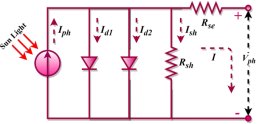
Figure 1. Representation of a Photovoltaic Solar Cell [2].
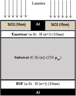
Figure 2. Schematic diagram of a heterojunction photovoltaic (PV) solar cell structure.
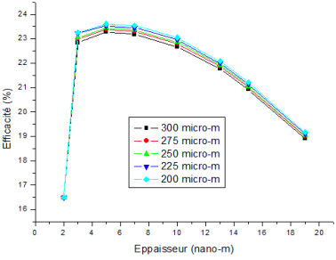
Figure 3. Impact of varying FSF layer thickness on cell efficiency.
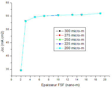
Figure 4. Impact of varying FSF layer thickness on cell current density.
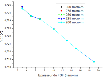
Figure 5. Impact of varying FSF layer thickness on cell open circuit voltage.
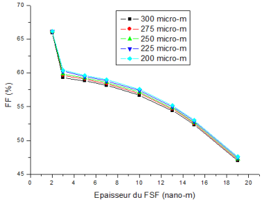
Figure 6. Impact of varying FSF layer thickness on cell form factor.
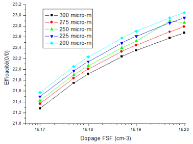
Figure 7. Evolution of cell efficiency as a function of FSF layer doping.
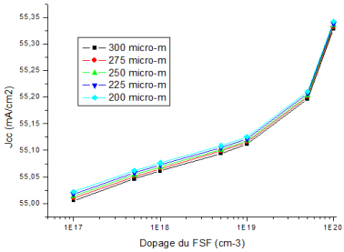
Figure 8. Evolution of cell current density as a function of FSF layer doping.
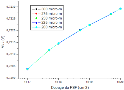
Figure 9. Evolution of cell open-circuit voltage as a function of FSF layer doping.
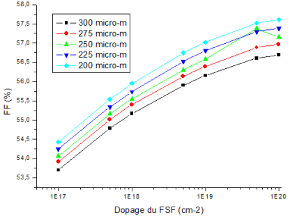
Figure 10. Evolution of cell form factor as a function of FSF layer doping.
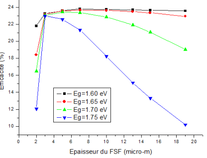
Figure 11. Evolution of Efficiency as a Function of FSF Thickness for Different Band gap Energies.
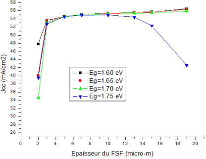
Figure 12. Evolution of the current density as a function of FSF thickness for different band gap energies.
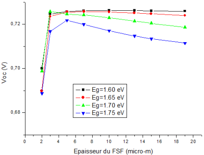
Figure 13. Open-circuit voltage variation as a function of FSF thickness for different band gap energies.
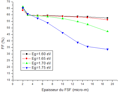
Figure 14. Form factor evolution as a function of FSF thickness for different bandgap energies.
Information

