Importance of renewable energy cannot be over emphasized. Titanium IV oxide (TiO2) is the most suitable semiconductor for dye sensitized solar cell (DSSC) due to its chemical stability, non toxicity and excellent optoelectronic properties. In this research TiO2 is coated on graphene to enhance its charge transport aiming to reduce recombination which is a main set back in DSSCs. undestanding graphene- TiO2 contact is therefore essential for DSSC application. TiO2 thin films were deposited on single layer graphene (SLG) as well as on flourine tin oxide (FTO) using doctor blading technique. The films were annealed at rates of 2°C /min and 1°C/min up to a temperature of 450°C followed by sintering at this temperature for 30 minutes. Four point probe SRM-232 was used to measure sheet resistance of the samples. The film thickness were obtained from transmittance using pointwise unconstrained minimization approximation (PUMA). UV –VIS spectrophotometer was employed to measure transmittance. Resistivity of TiO2 on both FTO and Graphene were of order 10-4 Ωcm. However, TiO2 annealed on graphene matrix exhibited a slightly lower resistivity 5.6 x10⁻⁴ Ωcm as compared to 6.0x10⁻⁴ Ωcm on FTO. Optical transmittance on visible region was lower for TiO2 on FTO than on SLG, 71.48% and 80.11% respectively. Urbach energy (Eu) for weak absorption region decreased with annealing rate. Urbach energies for 1°C/min TiO2 on FTO and SLG were 361 meV and 261meV respectively. This was used to account for decrease of disoders of films due to annealing. A striking relation between sheet resistivity and urbach was reported suggesting SLG as a suitable candidate for photoanode of a DSSC.
| Published in | Journal of Photonic Materials and Technology (Volume 10, Issue 1) |
| DOI | 10.11648/j.jmpt.20241001.12 |
| Page(s) | 7-12 |
| Creative Commons |
This is an Open Access article, distributed under the terms of the Creative Commons Attribution 4.0 International License (http://creativecommons.org/licenses/by/4.0/), which permits unrestricted use, distribution and reproduction in any medium or format, provided the original work is properly cited. |
| Copyright |
Copyright © The Author(s), 2024. Published by Science Publishing Group |
Graphene, Urbach Energy, Resistivity, Annealing, Titanium IV Oxide
Sample | Peak wavelength (λ) (nm) | Peak Transmittance (%) |
|---|---|---|
Graphene | 502.89 | 81.62 |
TiO2 on Graphene | 686.71 | 71.95 |
FTO | 746.43 | 80.28 |
TiO2 on FTO | 754.22 | 66.25 |
Urbach energy | 2o/ min | 1o/min |
|---|---|---|
Tio2 on FTO Eu (meV) | 414 | 365 |
TiO2 on Graphene(meV) | 329 | 260 |
FTO | Fourine Doped tin IV Oxide |
SLG | Single Layer Grapheme |
Gr | Grapheme |
1deg/min | One Degree Per Minute |
2deg/min | Two Degrees Per Minute |
Eu | Urbach Energy |
TiO2 | Titanium IV Oxide |
CVD | Chemical Vapour Deposition |
| [1] | Fuyuki T, Matsunami H. Electronic properties of the interface between Si and TiO2 deposited at very low temperatures. Jpn J Appl Phys 1986; 25: 1288. |
| [2] | Miao L Et al. Preparation and characterization of polycrystalline anatase and rutile TiO2 thin films by rf magnetron sputtering. Appl Surf Sci 2003; 212: 255. |
| [3] | Benjamin M. J., Simon W. M., and James M. N. (2018) “Effect of Annealing Rates on Surface Roughness of TiO2 Thin films.” Journal of Materials Physics and Chemistry, 6(2): 43-46. |
| [4] | R. Jose, V. Thavasi, and S. Ramakrishna, “Metal oxides for dye-sensitized solar cells,” Journal of the American Ceramic Society, vol. 92 (2), pp. 289-301, 2009. |
| [5] | Geim, A. K., & Novoselov, K. S. (2007). The rise of graphene. Nature materials, 6(3), 183-191. |
| [6] | K. S. Novoselov, A. K. Geim, S. V. Morozov, D. Jiang, Y. Zhang, S. V. Dubonos, I. V. Grigorieva, and A. A. Firsov, Electric field effect in atomically thin carbon films, Science, 306, 2004, 666–669. |
| [7] | Boubaker, K. A physical explanation to the controversial Urbach tailing universality. Eur. Phys. J. Plus 126, 10 (2011). |
| [8] | Biwas Subedi, Chongwen Li, Cong Chen, Dachang Liu, Maxwell M. Junda, Zhaoning Song, Yanfa Yan, and Nikolas J. PodrazaACS Applied Materials & Interfaces 2022 14 (6), 7796-7804. |
| [9] | Theiss, W. (2000). Scout thin films analysis software handbook, edited by Theiss M (Hand and Software Aachen German) www.mtheiss.com |
| [10] | Boubaker K. (2011). A physical explanation to the controversial Urbach tailing universality, The European Physics Journal Plus, 126, 10. |
| [11] | Ernesto G. Birgin, Ivan E. Chambouleyron, José Mario Martı́nez, Sergio D. Ventura, Estimation of optical parameters of very thin films, Applied Numerical Mathematics, 47, 2003, 109-119. |
| [12] | Ernesto G Birgin, Ivan Chambouleyron, José Mario Martı́nez, Estimation of the Optical Constants and the Thickness of Thin Films Using Unconstrained Optimization, Journal of Computational (1999) Physics, 151: 862880. |
| [13] | Larbah, Youssef & Rahal, Badis & Adnane, Mohamed. (2020).The effect of fluorine doping on the properties of SnO2 thin films deposited using spray pyrolysis method. Journal of Optoelectronics and Advanced Materials. 22. 518-522. |
| [14] | El-Nahass, M. M., Soliman, H. S., El-Denglawey, A. (2016). Absorption edge shift, opticalconductivity, and energy loss function of nano thermal-evaporated N-typeanatase TiO2 films. Appl Phys A; 122: 775. |
| [15] | Mathews, N. R., Morales, E. R., Cortés-Jacome, M. A., & Antonio, J. T. (2009). TiO2 thin films–Influence of annealing temperature on structural, optical and photocatalytic properties. Solar Energy, 83(9), 1499-1508. |
| [16] | Wibowo, K. M., Sahdan, M. Z., Asmah, M. T., Saim, H., Adriyanto, F., & Hadi, S. (2017), August). Influence of Annealing Temperature on Surface Morphological and Electrical Properties of Aluminum Thin Film on Glass Substrate by Vacuum Thermal Evaporator. In IOP Conference Series: Materials Science and Engineering (Vol. 226, No. 1, p. 012180). IOP Publishing. |
| [17] | Jayasinghe, Lihini., Jayaweera, Vimukthi., de Silva, Nuwan., Mubarak, Azeez M. Role of ZrO2 in TiO2 composites with rGO as an electron mediator to enhance the photocatalytic activity for the photodegradation of methylene blue. Materials Advances (2022) 3: 7904-7917. |
| [18] | Dilawar Ali, M. Z. Butt, Iqra Muneer, FarooqBashir, MurtazaSaleem. Correlation between structural andoptoelectronic properties of tin doped indium oxide thin films (2017). 128: 235-246. |
| [19] | Rahman, Md. (2023). Synthesis of CdS and CdTe Through A Novel Solution Process for Application in Thin Film Solar Cells. |
| [20] | Al-Shomara, S. M., Alahmad W. R. (2019), Annealing temperature effect on structural, optical and photocatalytic activity of nanocrystalline TiO2 films prepared by sol-gel method used for solar cell application, Digest Journal of Nanomaterials and Biostructures, 14, 617-625. |
APA Style
Riungu, G. G., Mugo, S. W., Ngaruyia, J. M., Gitu, L. (2024). Influence of Graphene on Sheet Resistivity and Urbach Enery of Nano TiO2 for DSSC Electrode. Journal of Photonic Materials and Technology, 10(1), 7-12. https://doi.org/10.11648/j.jmpt.20241001.12
ACS Style
Riungu, G. G.; Mugo, S. W.; Ngaruyia, J. M.; Gitu, L. Influence of Graphene on Sheet Resistivity and Urbach Enery of Nano TiO2 for DSSC Electrode. J. Photonic Mater. Technol. 2024, 10(1), 7-12. doi: 10.11648/j.jmpt.20241001.12
AMA Style
Riungu GG, Mugo SW, Ngaruyia JM, Gitu L. Influence of Graphene on Sheet Resistivity and Urbach Enery of Nano TiO2 for DSSC Electrode. J Photonic Mater Technol. 2024;10(1):7-12. doi: 10.11648/j.jmpt.20241001.12
@article{10.11648/j.jmpt.20241001.12,
  author = {Geoffrey Gitonga Riungu and Simon Waweru Mugo and James Mbiyu Ngaruyia and Leonard Gitu},
  title = {Influence of Graphene on Sheet Resistivity and Urbach Enery of Nano TiO2 for DSSC Electrode
},
  journal = {Journal of Photonic Materials and Technology},
  volume = {10},
  number = {1},
  pages = {7-12},
  doi = {10.11648/j.jmpt.20241001.12},
  url = {https://doi.org/10.11648/j.jmpt.20241001.12},
  eprint = {https://article.sciencepublishinggroup.com/pdf/10.11648.j.jmpt.20241001.12},
  abstract = {Importance of renewable energy cannot be over emphasized. Titanium IV oxide (TiO2) is the most suitable semiconductor for dye sensitized solar cell (DSSC) due to its chemical stability, non toxicity and excellent optoelectronic properties. In this research TiO2 is coated on graphene to enhance its charge transport aiming to reduce recombination which is a main set back in DSSCs. undestanding graphene- TiO2 contact is therefore essential for DSSC application. TiO2 thin films were deposited on single layer graphene (SLG) as well as on flourine tin oxide (FTO) using doctor blading technique. The films were annealed at rates of 2°C /min and 1°C/min up to a temperature of 450°C followed by sintering at this temperature for 30 minutes. Four point probe SRM-232 was used to measure sheet resistance of the samples. The film thickness were obtained from transmittance using pointwise unconstrained minimization approximation (PUMA). UV –VIS spectrophotometer was employed to measure transmittance. Resistivity of TiO2 on both FTO and Graphene were of order 10-4 Ωcm. However, TiO2 annealed on graphene matrix exhibited a slightly lower resistivity 5.6 x10⁻⁴ Ωcm as compared to 6.0x10⁻⁴ Ωcm on FTO. Optical transmittance on visible region was lower for TiO2 on FTO than on SLG, 71.48% and 80.11% respectively. Urbach energy (Eu) for weak absorption region decreased with annealing rate. Urbach energies for 1°C/min TiO2 on FTO and SLG were 361 meV and 261meV respectively. This was used to account for decrease of disoders of films due to annealing. A striking relation between sheet resistivity and urbach was reported suggesting SLG as a suitable candidate for photoanode of a DSSC.
},
 year = {2024}
}
TY  - JOUR
T1  - Influence of Graphene on Sheet Resistivity and Urbach Enery of Nano TiO2 for DSSC Electrode

AU  - Geoffrey Gitonga Riungu
AU  - Simon Waweru Mugo
AU  - James Mbiyu Ngaruyia
AU  - Leonard Gitu
Y1  - 2024/07/23
PY  - 2024
N1  - https://doi.org/10.11648/j.jmpt.20241001.12
DO  - 10.11648/j.jmpt.20241001.12
T2  - Journal of Photonic Materials and Technology
JF  - Journal of Photonic Materials and Technology
JO  - Journal of Photonic Materials and Technology
SP  - 7
EP  - 12
PB  - Science Publishing Group
SN  - 2469-8431
UR  - https://doi.org/10.11648/j.jmpt.20241001.12
AB  - Importance of renewable energy cannot be over emphasized. Titanium IV oxide (TiO2) is the most suitable semiconductor for dye sensitized solar cell (DSSC) due to its chemical stability, non toxicity and excellent optoelectronic properties. In this research TiO2 is coated on graphene to enhance its charge transport aiming to reduce recombination which is a main set back in DSSCs. undestanding graphene- TiO2 contact is therefore essential for DSSC application. TiO2 thin films were deposited on single layer graphene (SLG) as well as on flourine tin oxide (FTO) using doctor blading technique. The films were annealed at rates of 2°C /min and 1°C/min up to a temperature of 450°C followed by sintering at this temperature for 30 minutes. Four point probe SRM-232 was used to measure sheet resistance of the samples. The film thickness were obtained from transmittance using pointwise unconstrained minimization approximation (PUMA). UV –VIS spectrophotometer was employed to measure transmittance. Resistivity of TiO2 on both FTO and Graphene were of order 10-4 Ωcm. However, TiO2 annealed on graphene matrix exhibited a slightly lower resistivity 5.6 x10⁻⁴ Ωcm as compared to 6.0x10⁻⁴ Ωcm on FTO. Optical transmittance on visible region was lower for TiO2 on FTO than on SLG, 71.48% and 80.11% respectively. Urbach energy (Eu) for weak absorption region decreased with annealing rate. Urbach energies for 1°C/min TiO2 on FTO and SLG were 361 meV and 261meV respectively. This was used to account for decrease of disoders of films due to annealing. A striking relation between sheet resistivity and urbach was reported suggesting SLG as a suitable candidate for photoanode of a DSSC.

VL  - 10
IS  - 1
ER  -
Department of Physics, College of Pure and Applied Sciences, Jomo Kenyatta University of Agriculture and Technology, Nairobi, Kenya
Department of Physics, College of Pure and Applied Sciences, Jomo Kenyatta University of Agriculture and Technology, Nairobi, Kenya
Department of Physics, College of Pure and Applied Sciences, Jomo Kenyatta University of Agriculture and Technology, Nairobi, Kenya
Department of Chemistry, College of Pure and Applied Sciences, Jomo Kenyatta University of Agriculture and Technology, Nairobi, Kenya
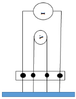
Figure 1. Functional block diagram of SRM-232 Four-point probe.
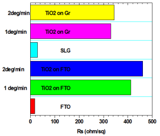
Figure 2. Sheet resistance for annealed TiO2 on FTO and Graphene films.
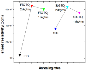
Figure 3. Sheet resistivity against annealing for TiO2 on FTO and grapheme.
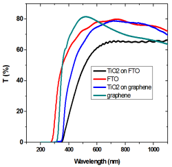
Figure 4. Transmittance for annealed TiO2 on graphene and FTO versus wavelength.
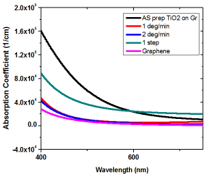
Figure 5. Absorption coefficient for as deposited and annealed TiO2 films on Graphene.
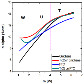
Figure 6. ln (α) vs (hυ) for annealed TiO2 on Graphene and FTO.
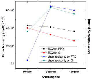
Figure 7. A relation between Urbach energies and resistivity for TiO2 on FTO and graphene.
Information

